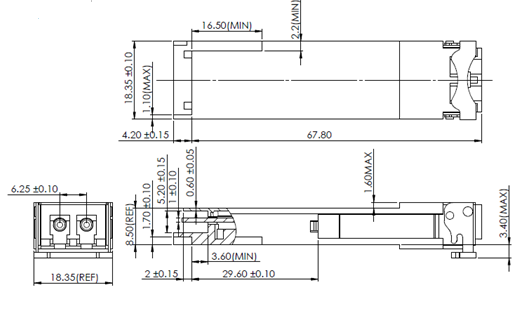
- 4 CWDM lanes MUX/DEMUX design
- 4 independent full-duplex channels Up to 11.2Gbps data rate per wavelength
- 4 CWDM channels are 1271, 1291, 1311 and 1331 nm
- Single +3.3V power supply
- QSFP+ MSA compliant
- Up to 10km transmission
- Operating case temperature: 0~70C
- Maximum 3.5W operation power
- RoHS compliant
- Compliant with IEEE802.3ba
- Compliant with QSFP+ MSA: SFF-8436
- The Quad (4-channel) Small Form-factor Pluggable (often abbreviated as QSFP or QSFP+) is a compact, hot-pluggable transceiver used for data communications applications. It interfaces a network device motherboard (for a switch, router, media converter or similar device) to a fiber optic cable. It is an industry format jointly developed and supported by many network component vendors, supporting data rates from 4x10 Gb/s. The format specification is evolving to enable higher data rates model specified here offers 40G datarate over 4 independent full-duplex channels Up to 11.2Gbps data rate per wavelength
- The QSFP specification supports Ethernet, Fiber Channel, InfiniBand and SONET/SDH standards with different data rate options. QSFP+ transceivers are designed to support Serial Attached SCSI, 40G Ethernet, 20G/40G Infiniband, and other communications standards. QSFP modules increase the port-density by 3x-4x compared to SFP+ modules.

40G QSFP transceiver module general specifications
Absolute Maximum Ratings
Parameter
Symbol
Min
Max
Unit
Note
Storage Temperature
TS
-40
85
°C
Relative Humidity
RH
0
85
%
Supply Voltage
Vcc
-0.5
4.0
V
Recommended Operating Conditions
Parameter
Symbol
Min
Typ
Max
Unit
Note.
Power Supply Voltage Vcc
3.13
3.30
3.47
V
Power Supply Current Icc
-
-
100
mA
Case Operating Temperature Tc
-5
-
+70
°C
Optical Characteristics
Parameter
Symbol
Min.
Typical
Max
Unit
Notes
Wavelength Assignment
L0
1264.5
1271
1277.5
nm
L1 1284.5 1291 1297.5 nm L2 1304.5 1311 1317.5 nm L3 1324.5 1331 1337.5 nm Transmitter Side-mode Suppression Ratio
SMSR
30
-
-
dB
Total Average Launch Power
PT
-
-
8.3
dBm
Average Launch Power, each Lane
-7
-
2.3
dBm
Optical Modulation Amplitude, each Lane
OMA
-4
-
+3.5
dBm
Difference in Launch Power between any two Lanes (OMA)
-
-
6.5
dB
Launch Power in OMA minus Transmitter and Dispersion Penalty (TDP), each Lane
-4.8
-
dBm
TDP, each Lane
TDP
2.3
dB
Extinction Ratio
ER
3.5
-
-
dB
Relative Intensity Noise
Rin
-
-
-128
dB/Hz
12dB reflection
Optical Return Loss Tolerance
-
-
20
dB
Transmitter Reflectance
RT
-12
dB
Transmitter Eye Mask Definition {X1, X2, X3, Y1, Y2, Y3}
{0.25,0.4,0.45,0.25,0.28,0.4}
Average Launch Power OFF Transmitter, each Lane
Poff
-30
dBm
Receiver Damage Threshold
THd
3.3
dBm
1
Average Power at Receiver Input, each Lane
-13.7
2.3
dBm
Receiver Reflectance
RR
-
-
-26
dB
Receiver Power (OMA), each Lane
-
-
3.5
dBm
Stressed Receiver Sensitivity in OMA, each Lane
-
-
-9.9
dBm
Receiver Sensitivity, each Lane
SR
-
-
-11.5
dBm
Difference in Receive Power between any two Lanes (OMA)
7.5
dB
Conditions of Stress Receiver Sensitivity Test2 Vertical Eye Closure Penalty, each Lane
1.6
dB
Stressed Eye Jitter, each Lane
0.3
UI
Notes:
- The receiver shall be able to tolerate, without damage, continuous exposure to a modulated optical input signal having this power level on one lane. The receiver does not have to operate correctly at this input power.
- Vertical eye closure penalty and stressed eye jitter are test conditions for measuring stressed receiver sensitivity. They are not characteristics of the receiver.
Electrical Characteristics
Parameter
Symbol
Min.
Typical
Max
Unit
Notes
Data Rate, each Lane - 10.3125 11.2 Gbps Power Consumption (XLPPI) - 1.5 W Supply Current ICC 0.75 1.0 A Control I/O Voltage, High VIH 2.0 VCC V Control I/O Voltage, Low VIL 0 0.7 V Inter-Channel Skew TSK 150 ps RESETL Duration 10 us RESETL De-assert time 100 ms Power on time 100 ms Transmitter (XLPPI)
Single Ended Output Voltage Tolerance -0.3 - 4 V Referred to signal common AC Common mode Voltage Tolerance (RMS) 15 - - mV Tx Input Diff Voltage VI 90 1600 mV Tx Input Diff Impedance ZIN 80 100 120 W Differential Input Return Loss See IEEE 802.3ba 86A.4.11 dB 10MHz- 11.1GHz J2 Jitter Tolerance Jt2 0.18 UI J9 Jitter Tolerance Jt9 0.26 UI Data Dependent Pulse Width Shrinkage DDPWS 0.07 UI Eye Mask Coordinates {X1, X2
Y1, Y2} 0.1, 0.31
95, 350UI
mVReceiver (XLPPI)
Single Ended Output Voltage Tolerance1 -0.3-4VReferred to TP1 signal commonAC Common mode Voltage Tolerance (RMS) --7.5mV Termination Mismatch at 1MHz 5% Differential Output Return Loss See IEEE 802.3ba 86A.4.2.1dB10MHz- 11.1GHzCommon-mode Output Return Loss See IEEE 802.3ba 86A.4.2.2dB10MHz- 11.1GHzRx Output Diff VoltageVo 600800mV Rx Output Rise and Fall TimeTr/Tf 35ps20% to 80%J2 Jitter ToleranceJr2 0.46UI J9 Jitter ToleranceJr9 0.63UI Eye Mask Coordinates {X1, X2
Y1, Y2} 0.29, 0.5
150, 425UI
mV
Notes:1. The single ended input voltage tolerance is the allowable range of the instantaneous input signals